Microsoft Just Acquired a Chip Design Start-Up Here's What Semiconductor Investors Need to Know. The Motley Fool
Table Of Content

The Protium X3 platform for emulation uses AMD Field Programmable Gate Arrays (FPGAs) to test software on the design validated by the Palladium. I'll reiterate here that semiconductor investors shouldn't worry too much about Microsoft's latest acquisition. Fungible is a tiny start-up, and it's unlikely to completely displace Microsoft's chip supply partners anytime soon. However, big tech's growing interest in designing chips is real. In this step, the conversion of the netlist to its geometric representation is realized, and the result is called the layout, which can verify the synthesized netlist functionally.
Archer Miniaturises Biochip gFET Chip Design - Business Wire
Archer Miniaturises Biochip gFET Chip Design.
Posted: Thu, 14 Mar 2024 07:00:00 GMT [source]
Advertise with MIT Technology Review
But what is one thing that I even mentioned last time, what is different from 2018 to now, is that EDA and IP is much more valuable to the industry. And in that part, as they design bigger and bigger chips, because the big thing in AI systems is they are parallel. So the tools have to be more efficient, the hardware platform have to support that. So we're using all our latest tools, all the latest AI tools, we are using all our IP. There's a very good validation of our own capabilities that we can accelerate our design process, but really sets up hardware verification and overall verification flow for using the new systems. Our Digital IC business had another solid quarter as our digital full flow continued to proliferate at the most advanced nodes.

Baby Photos App
There are a ton of templates, fonts images, many of which are free to use. Canva works on the drag and drop concept, where you only need to select the elements and drag it to your work area and customize it. Adobe Photoshop is arguably the most popular graphic design software and is used by millions of artists around the world.
Extended data figures and tables
More Taiwan IC design businesses leaving entry-level market in China - DIGITIMES
More Taiwan IC design businesses leaving entry-level market in China.
Posted: Wed, 24 Apr 2024 01:42:29 GMT [source]
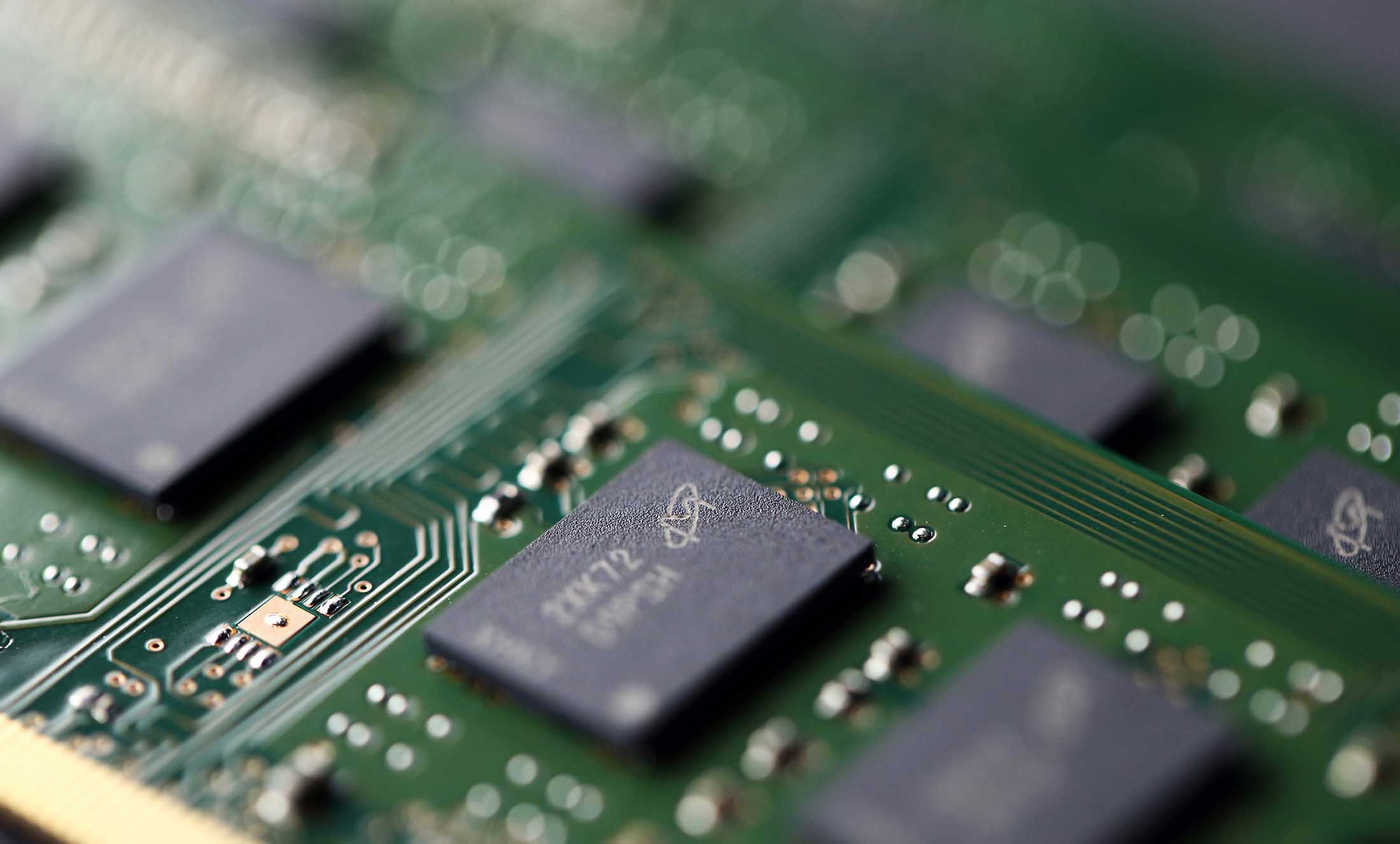
Slight changes to the amount of diffusion time, uneven doping levels, etc. can have large effects on device properties. Integrated circuit design involves the creation of electronic components, such as transistors, resistors, capacitors and the interconnection of these components onto a piece of semiconductor, typically silicon. A method to isolate the individual components formed in the substrate is necessary since the substrate silicon is conductive and often forms an active region of the individual components.
Extended Data Fig. 3 Generalization performance as a function of pre-training dataset size.
India's semiconductor ambitions have made huge strides with Prime Minister Narendra Modi's government approving three semiconductor plants in Gujarat and Assam with investments of more than $15 billion. The Palladium Z3 helps debug the hardware while the FPGA-based Protium X3 emulates the hardware ... Fungible also has a product called the Storage Cluster that helps data center operators with data storage challenges. All on its own, Microsoft acquiring a small company like Fungible doesn't add up. But a wave of disruption could be coming to the semiconductor industry. Develop Boolean expressions, control flow, word width, register allocation, etc., and use VHDL or Verilog HDL hardware description language to describe functions in codes to form register transfer level (RTL) codes.
Productization
This step follows some predefined fixed rules, such as the lambda rule, which provides exact details such as component size, scale, and spacing. The next step is to verify the functions and timing of the physical layout of the completed wiring. The verification items usually include LVS, DRC, ERC, etc., and of course some power consumption analysis and manufacturability analysis. A customer of a semiconductor firm is typically some other company who plans to use the chip in their systems or end products. So, requirements of the customer also play an important role in deciding how the chip should be designed.
conversations with readers and editors. For more exclusive content and features, consider
Next, turning to the balance sheet and cash flow, cash balance at quarter end was [$1.012 billion] (ph). While the principal value of debt outstanding was $650 million. DSOs were 36 days and we used $125 million to repurchase Cadence shares in Q1. I am pleased to report that Cadence delivered strong results for the first quarter of 2024. First quarter bookings were a record for Q1 and we achieved record Q1 backlog of approximately $6 billion. A good start to the year coupled with some impressive new product launches, sets us up for strong growth momentum in the second half of 2024.
Analogy of Chip Design Architecture Vs Building Architecture.[edit edit source]
You can define the size of your canvas, isolate elements from backgrounds, create custom brushes, work in 3D, do much more. "When heat crosses a boundary from one material to another, there's typically some slowdown to get into the next material," Hu said. "The key feature in our boron arsenide material is its very low thermal- boundary resistance. This is sort of like if the heat just needs to step over a curb, versus jumping a hurdle."
And our customers are fully embracing both these systems as they invariably do both chip development and software development. I mean, perfect example is of course, our long-term development partner, NVIDIA. Ever-increasing complexities in the system verification and software bring-up continue to propel the demand of our functional verification products.
But the design activity in China remains very strong, though. I mean Q1 IP performance and bookings were ahead of our expectations. And everything remains on track there for a very strong growth year for 2024 for the IP business. We're pleased with the overall business momentum, but we need to scale up some headcounts to prepare to deliver on some of the larger backlog orders. And now we do use, you know, products like InfiniBand in our systems on Z3 to your question, which is, because Z3 is a very unique architecture. Now in X3, we are using AMD FPGAs, which are fabulous, but it does not require that tight interconnect speed.
Additionally, Cadence's cloud native molecular design platform, Orion, will be supercharged with NVIDIA's BioNemo and NVIDIA microservices for drug discovery to broaden therapeutic design capabilities and shorten time to trusted results. Building upon the successes of the industry leading Z2, X2 systems, this new platform set a new standard of excellence, delivering more than twice the capacity and 50% higher performance per rack than the previous generation. Palladium Z3 is powered by our next generation custom processor and was designed with Cadence AI tools and IP. The Z3 system is future proof with its massive 48 billion gate capacity, enabling emulation of the industry's largest design for the next several generations. Generative AI is reshaping the entire chip and system development process.
Define the basic specifications of the system, such as floating-point units; determine the system to be used, such as reduced instruction set computer (RISC) or complex instruction set computer (CISC); finalize the number of ALU cache sizes, etc. Much of the work being done in the industry is proprietary. Skepticism presents another challenge, as there are engineers who question how a machine could possibly derive better results than they can. Synthesizable assertions are mapped to emulators to perform at system speeds. Ensure that the design has spare functional gates well distributed across the layout. Ensure that the selection the spare gates, has many flavours of gates and universal gates, so that any functionality could be achieved.
The next and most important step is to translate the system to physical level. At this level, the schematic is converted into physical layout using basic building blocks. For example, the below diagram shows the layout of a two input AND gate which was shown above. We can observe that each transistor is replaced with the corresponding physical layout, while the interconnects are replaced with different metal layers like Metal 1, Metal 2 and Polysilicon. This seems to be a bit complex process, as the designer has to make all the transistors and interconnects by hand. Finally, IP cores are very important for chip design process.
The unique thing about Visme is you can bring your content to life with advanced animation and interactivity features. For example, you can create a custom animated character, or add links, hover effects and pop-ups to your designs. GIMP is a free graphic design program that works on many platforms like Windows, Linux, and Mac OS.
By understanding the requirements of each stage, chip designers can create efficient, reliable, and cost-effective designs that meet the need of their customers across various industrial domains. The first step in any new development involves determining the type of device/product to be designed, such as an integrated circuit (IC), ASIC, FPGA, SoC, and others. For instance, if the aim is to create something small yet powerful enough for high-speed applications like telecommunications or networking equipment, the best option might be an Application-Specific Integrated Circuit (ASIC). If the goal is to design something more flexible, capable of performing multiple tasks with minimal overhead, then an FPGA could be a better choice. Once the device type is chosen, the specifications can be defined. Next, this basic design is used to create a logic circuit (electronic circuit) using a special computer language to describe and model digital circuits.


Comments
Post a Comment